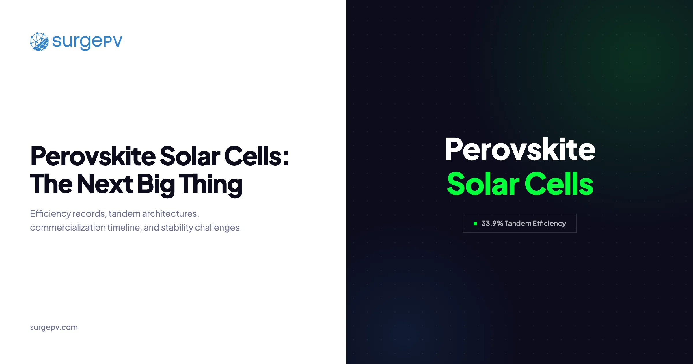
In November 2023, LONGi Green Energy published a certified efficiency of 33.9% for its perovskite-silicon tandem solar cell — a number that crossed a threshold the photovoltaic industry had been chasing for two decades. For context, the best commercial silicon panel you can buy today converts roughly 22–24% of sunlight into electricity. That single data point explains why every major solar manufacturer, national laboratory, and venture capital fund is now betting heavily on perovskite.
Yet for solar installers and developers pricing projects today in 2026, perovskite panels are not on any distributor’s shelf at scale. The gap between a certified lab record and a 25-year outdoor-warranted product is enormous, and most reporting on perovskite conflates the two. This guide separates them — with real efficiency data from NREL, Fraunhofer ISE, and the major research consortia, a clear-eyed look at what is actually shipping, and a realistic commercial timeline that accounts for the durability challenges that remain unsolved.
TL;DR — Perovskite Solar Cells in 2026
Single-junction perovskite: 26.7% certified (KAUST, 2024). Perovskite-silicon tandem: 33.9% certified (LONGi, 2023). First commercial tandem products are emerging from Oxford PV and Saule Technologies, but mainstream installer-grade perovskite panels with full 25-year warranties are still 2–4 years out. Lead-free tin perovskite has reached 15.1% efficiency. The technology is real, the efficiency gains are verified, and the commercialization clock is running — but silicon is not obsolete yet.
What you will learn in this guide:
- The ABX3 crystal structure that makes perovskite uniquely efficient and uniquely unstable
- Every major certified efficiency record as of early 2026, sourced from the NREL chart and Fraunhofer ISE
- How perovskite-silicon tandem cells break the single-junction efficiency ceiling
- Quantified degradation data: what moisture, UV, and thermal cycling actually do to perovskite
- Lead-free perovskite: current efficiency, toxicity risk, and the timeline to viability
- Manufacturing at scale: roll-to-roll printing vs. vapor deposition economics
- Which companies are closest to commercial volume: Oxford PV, Saule Technologies, Swift Solar
- A realistic 2026–2032 commercialization timeline
- What this means for solar installers specifying systems today
Latest Updates: Perovskite Solar Technology 2026
The table below summarizes the key certified efficiency records as of early 2026. All figures are independently certified; lab-claimed but uncertified values are excluded.
Certified Perovskite Efficiency Records — 2026
| Cell Type | Certified Efficiency | Institution / Company | Year Certified | Source |
|---|---|---|---|---|
| Perovskite single-junction (small area) | 26.7% | KAUST (King Abdullah Univ.) | 2024 | NREL Chart |
| Perovskite single-junction (1 cm²) | 25.7% | EPFL / CSEM | 2023 | NREL Chart |
| Perovskite-silicon tandem (2-terminal) | 33.9% | LONGi Green Energy | 2023 | Fraunhofer ISE cert. |
| Perovskite-silicon tandem (4-terminal) | 32.5% | HZB (Helmholtz-Zentrum Berlin) | 2023 | NREL Chart |
| Perovskite-silicon tandem (module, >800 cm²) | 26.8% | Oxford PV | 2023 | Oxford PV press release, Fraunhofer cert. |
| All-perovskite tandem (2-terminal) | 28.0% | MIT / Brown University | 2023 | NREL Chart |
| Tin-lead perovskite (lead-free direction) | 22.0% | Monash University | 2024 | Nature Energy |
| Tin-only perovskite (truly lead-free) | 15.1% | Linköping University | 2023 | NREL Chart |
| Perovskite mini-module (>20 cm²) | 23.3% | EPFL | 2022 | NREL Chart |
Sources: NREL Best Research-Cell Efficiency Chart (version Jan 2026); Fraunhofer ISE certified test results; cited journal publications. Efficiencies measured under AM1.5G, 100 mW/cm², 25°C standard test conditions unless noted.
Three numbers in this table define the current state of play. The 26.7% single-junction record shows that perovskite has definitively outpaced silicon’s single-junction theoretical limit of ~29.4% Shockley-Queisser — there is still headroom, but not unlimited. The 33.9% tandem record demonstrates that stacking perovskite and silicon genuinely breaks through the single-junction ceiling. And the 26.8% module-scale result from Oxford PV is the one that matters most commercially — it shows that efficiency does not collapse catastrophically when moving from a 1 cm² research cell to a commercial-size substrate.
What Perovskite Actually Is: The ABX3 Crystal Structure
The word “perovskite” refers to a crystal structure, not a specific chemical compound. The general formula is ABX3, where:
- A is a large cation — typically methylammonium (MA⁺), formamidinium (FA⁺), or cesium (Cs⁺)
- B is a small metal cation — most commonly lead (Pb²⁺), increasingly tin (Sn²⁺)
- X is a halide anion — iodide (I⁻), bromide (Br⁻), or chloride (Cl⁻)
The canonical high-efficiency perovskite is methylammonium lead iodide: CH₃NH₃PbI₃ (MAPbI₃). You can visualize the structure as a three-dimensional grid of corner-sharing lead-iodide octahedra [PbI₆]⁴⁻, with the methylammonium cation sitting in the cage formed by eight of those octahedra.
Why This Structure Is Special
What makes the ABX3 perovskite structure so photovoltaically attractive is a combination of properties that silicon achieves only partially and that organic thin-films fail to combine at all:
Tunable bandgap. By substituting different A-site cations or mixing halides (e.g., iodide-bromide blends), you can tune the optical bandgap continuously from roughly 1.2 eV to 3.0 eV. Silicon has a fixed bandgap of 1.12 eV. This tunability is what enables tandem cell design — you can engineer a perovskite layer with a bandgap of exactly 1.68 eV to complement silicon’s 1.12 eV, dividing the solar spectrum optimally between the two absorbers.
High absorption coefficient. Perovskite absorbs photons roughly 10× more efficiently than crystalline silicon per unit thickness. A 500 nm perovskite film captures most above-bandgap photons; silicon requires 180–300 μm. This is why perovskite cells can in principle be manufactured with far less material.
Long carrier diffusion lengths despite solution processing. In a high-quality silicon solar cell, electrons and holes must be kept alive long enough to reach the contacts — this requires ultrapure, precisely doped silicon grown at 1,400°C. Perovskites achieve diffusion lengths of 1–10 μm even when deposited from low-temperature solution processes, because defects in the perovskite lattice are surprisingly “benign” — they do not trap carriers as aggressively as equivalent defects in silicon or III-V semiconductors.
Low formation energy. The ionic bonding in ABX3 perovskite means the material can be deposited from precursor solutions at temperatures below 150°C, using spin-coating, blade coating, or slot-die coating. Compare that to silicon’s 1,400°C crystal growth or CdTe’s 600°C vapor deposition. Low processing temperature is the fundamental reason perovskite could ultimately be cheaper per watt than silicon — even at comparable efficiency.
The downside of low formation energy. The same ionic nature that enables cheap deposition also makes the crystal unstable. Water molecules, UV photons, and heat can break the A-site cation free and decompose the crystal. This is the central challenge of perovskite commercialization, and we address it in detail below.
Key Takeaway — Why Perovskite Outperforms Silicon in the Lab
Perovskite’s ABX3 crystal structure allows bandgap engineering, high optical absorption, and solution-phase deposition at under 150°C — three properties silicon cannot match simultaneously. These are structural advantages, not incremental improvements. They explain why perovskite went from 3.8% efficiency in 2009 to 26.7% in 2024, a pace of improvement that took silicon 40 years to achieve in its first comparable efficiency range.
Why Efficiency Matters: The Solar Learning Curve vs. Silicon’s Limits
To understand why the industry cares so much about perovskite, you need to understand where silicon’s efficiency stands against its physical ceiling — and what happens to economics when you push past that ceiling.
Silicon’s Efficiency Plateau
Commercial monocrystalline PERC (Passivated Emitter and Rear Contact) silicon panels peaked at around 22–23% in production around 2022–2023. TOPCon (Tunnel Oxide Passivated Contact) modules are now shipping at 23–24%. HJT (Heterojunction) panels from manufacturers like REC and Panasonic reach 24–25% in production. The single-junction silicon record, held by Kaneka’s HJT cell, stands at 29.1% — within about 0.3% of the theoretical Shockley-Queisser limit for silicon.
The industry is essentially done with single-junction silicon improvement. Going from 24% to 25% in production requires billions in R&D and manufacturing retooling for a 4% relative gain. The learning curve on silicon cost-per-watt — which has been extraordinarily productive since 1977, dropping ~20% for every doubling of cumulative production volume — is now dominated by scale economies and raw material costs, not efficiency improvements.
What Higher Efficiency Does to Economics
Higher efficiency panels produce the same power from a smaller area. When land, racking, wiring, and labor are significant cost components — as they are in commercial and utility-scale installations — efficiency improvements beyond silicon’s plateau translate directly to lower system cost per watt-peak, not just per panel.
A 35% efficient panel produces roughly 45% more power from the same footprint as a 24% panel. For a 1 MW commercial rooftop where space is genuinely constrained, that difference can mean the project is feasible or not. For utility-scale ground-mount, where land is a real cost, the balance-of-system savings on a 33% tandem system over a 22% PERC system can exceed $0.10/Wp — more than the current total panel cost for some commodity modules.
This is the core economic argument for tandem perovskite-silicon: not that it replaces silicon immediately, but that it lifts the efficiency ceiling in a way that improves whole-system economics even at a per-panel cost premium.
To understand how these technologies interact, it is worth reviewing the fundamentals in our guide on how solar panels work and what efficiency gains mean in practice.
Tandem Perovskite-Silicon Cells: Architecture, Records, and Key Players
Tandem solar cells are not new. The concept of stacking multiple semiconductor absorbers to capture different portions of the solar spectrum dates to the 1970s, and III-V multijunction cells (gallium arsenide, indium phosphide) have achieved efficiencies above 47% under concentrated light for decades. The problem is that III-V tandems cost $50,000/m² or more — viable for satellites and concentrating solar, not for rooftops.
Perovskite changes the tandem economics equation because it can be deposited cheaply on top of silicon by solution process, adding roughly $0.10–0.30/Wp in estimated production cost for potentially 10+ percentage points of efficiency gain.
Two-Terminal vs. Four-Terminal Architectures
Two-terminal (2T) tandems monolithically integrate the perovskite top cell and silicon bottom cell into a single device. Current flows in series through both layers. This requires current matching — both cells must generate the same number of charge carriers — which demands careful bandgap engineering and light management. The LONGi 33.9% record is a 2T device. 2T tandems are preferred for commercial manufacturing because they can be processed in a single production line, similar to adding a deposition step to a silicon cell line.
Four-terminal (4T) tandems keep the top and bottom cells electrically separate, each with its own contacts. Light passes through the perovskite top cell and the transmitted photons hit the silicon bottom cell. 4T avoids the current-matching constraint and is easier to optimize independently, but requires more processing steps and a transparent rear contact. The HZB 32.5% record is a 4T device.
For commercial manufacturing, 2T is the primary architecture being pursued by all major players.
Key Companies and Their Tandem Records
LONGi Green Energy (China)
LONGi is the world’s largest solar manufacturer by shipment volume. Its November 2023 announcement of 33.9% certified tandem efficiency — independently verified by Germany’s Fraunhofer ISE — was the most significant perovskite milestone of the year. LONGi has not publicly disclosed its precise cell architecture or the specific perovskite composition, citing competitive reasons. The company has stated publicly that commercialization of tandem products is a strategic priority, but has not given a firm product launch date as of early 2026.
Oxford PV (UK/Germany)
Oxford PV is the company furthest along on the manufacturing pathway for 2T perovskite-silicon tandems. Spun out of Oxford University in 2010, the company built a dedicated perovskite-silicon tandem cell production facility in Brandenburg an der Havel, Germany. Oxford PV’s key claim: a certified module efficiency of 26.8% on a commercial-size (>800 cm²) substrate — the largest area perovskite-silicon tandem module record. The company has also held the world record for 28% efficiency on a standard 6-inch silicon wafer format in 4T configuration.
Oxford PV raised £150 million from investors including Meyer Burger and the UK government’s British Business Bank. The Brandenburg facility was designed for a production target of approximately 125 MW/year initially, scaling toward GW capacity. As of early 2026, the company is in ramp phase, with early commercial deliveries underway. The modules use a silicon heterojunction (HJT) bottom cell paired with a solution-processed perovskite top cell.
HZB (Helmholtz-Zentrum Berlin, Germany)
HZB is not a commercial company but the German national research center that has consistently held or tied for the tandem efficiency world record. HZB’s 32.5% certified efficiency in 4T configuration and contributions to 2T architectures have been critical to the field. HZB collaborates closely with industry, including through the German government-funded PEROSEED and CAPITANO research programs.
KAUST (King Abdullah University of Science and Technology, Saudi Arabia)
KAUST holds the single-junction perovskite cell record of 26.7% (2024), certified by NREL. The KAUST group, led by Professor Stefaan De Wolf, has been particularly active in large-area deposition techniques and has published extensively on blade-coating methods scalable to industrial formats. KAUST’s work is relevant because Saudi Arabia’s Public Investment Fund has expressed interest in funding perovskite manufacturing — potentially creating a new geography for tandem production outside China and Europe.
Swift Solar (USA)
Swift Solar is an American startup developing all-perovskite tandem cells — stacking two perovskite layers rather than perovskite on silicon. The theoretical advantage is that all-perovskite tandems could in principle be manufactured entirely by solution-phase processes, without any silicon cell production. Swift raised $7 million in seed funding (2020) and additional Series A capital in 2022. The company targets the flexible and BIPV (building-integrated PV) markets where silicon tandems cannot go due to rigidity and weight constraints. All-perovskite tandems have reached 28.0% certified efficiency (MIT/Brown University, 2023), but manufacturing challenges for the tin-lead bottom cell remain significant.
Saule Technologies (Poland)
Saule is the most commercially active perovskite company in Europe, having deployed building-integrated perovskite modules at multiple real-world sites since 2021. The company’s founder, Olga Malinkiewicz, pioneered inkjet-printed perovskite deposition in 2013 while at the University of Valencia. Saule’s current products are single-junction perovskite modules, not tandems — efficiency is in the 13–15% range for installed modules — but the company has demonstrated real-world outdoor operation for multiple years, generating durability data that the industry urgently needs. Saule has a manufacturing partnership with Skanska for BIPV applications and has deployed installations in Poland and Japan.
Pro Tip — What to Watch for in Tandem Product Specs
When evaluating tandem panel announcements, look for three numbers: certified module efficiency (not cell efficiency, and not lab efficiency on a 1 cm² sample), temperature coefficient (perovskite-silicon tandems typically show -0.25 to -0.30%/°C vs. -0.35 to -0.45%/°C for standard silicon — a real performance advantage in hot climates), and the IEC 61215 and IEC 61730 certification status. Without those certifications, the product cannot be legally installed in most markets and is not bankable for project finance.
Stability Challenges: Moisture, UV, and Heat Degradation
This is the section that separates perovskite from a laboratory curiosity — and the one where honest reporting is most needed. Perovskite cells degrade. The question is how fast, under what conditions, and whether the degradation can be brought within the range required for a 25-year outdoor warranty.
The Three Primary Degradation Pathways
Moisture degradation. Water molecules attack the A-site methylammonium cation in MAPbI₃, breaking the hydrogen bond network and causing the crystal to decompose to lead iodide (PbI₂), which is photoelectrochemically inactive. Even ambient humidity at 30–40% RH can cause measurable degradation in unencapsulated perovskite cells within hours. Modern perovskite cells use multiple mitigation strategies: replacing MA⁺ with more stable FA⁺ or Cs⁺, mixed-cation compositions (e.g., FA₀.₈₃Cs₀.₁₇PbI₃), and aggressive encapsulation with moisture barrier films (typically Al₂O₃ or SiN multilayers deposited by atomic layer deposition).
UV degradation. Ultraviolet photons carry enough energy to break Ti-O bonds in TiO₂, a common electron transport layer in early perovskite cells, generating reactive oxygen species that attack the perovskite layer. This was a major early stability problem. The field has largely moved away from TiO₂ to UV-stable alternatives: SnO₂ (tin oxide) as an electron transport layer is now standard in high-stability architectures. Spiro-OMeTAD, the dominant hole transport material, also degrades under UV — dopant-free alternatives including PTAA and polymeric HTLs are being validated.
Thermal degradation (thermomechanical fatigue). Perovskite cells are tested under IEC 61215 thermal cycling between -40°C and +85°C, repeated 200 times. The mismatch in thermal expansion coefficients between the perovskite film, transport layers, and glass or silicon substrate generates mechanical stress at interfaces. FA-based and mixed-halide compositions show substantially better thermal stability than MAPbI₃ due to their higher decomposition temperature (~240°C vs. ~150°C for MAPbI₃).
What the Durability Data Actually Shows
EPFL Damp Heat Results (2023). The EPFL group published results in Nature Energy showing that optimized FA-Cs perovskite cells with SnO₂ electron transport and PTAA hole transport retained >90% of initial efficiency after 1,000 hours of damp-heat testing at 85°C/85% RH. The IEC 61215 standard requires performance retention after 1,000 hours of damp heat. This was the first time a perovskite cell passed an analog of the IEC damp-heat test — a significant milestone.
LONGi’s tandem stability data. LONGi has not published detailed stability datasets for its 33.9% record cell, which is typical for competitive reasons. The company has stated publicly that its tandem development roadmap includes stability qualification as a prerequisite for commercial launch.
Oxford PV module field data. Oxford PV has the most commercially relevant stability dataset because its modules have been deployed in outdoor test installations. The company has disclosed that modules in its Brandenburg pilot line showed less than 3% degradation in first-year outdoor testing — comparable to silicon panel degradation rates. However, “first year” is a very different standard from “25 years.” Long-term extrapolation from accelerated aging tests remains an active area of scientific debate.
Saule Technologies field deployment data. Saule’s BIPV modules deployed in 2021 in Wrocław, Poland have now completed approximately 4 years of outdoor operation as of early 2026. The company has disclosed that the modules are still operating within specification, but has not published detailed performance degradation curves. The operating environment for BIPV (shaded from direct rain, lower irradiance) is less stressful than standard rooftop conditions.
The 25-year gap. IEC 61215 was designed for silicon panels that have an established 30-year track record. Its accelerated aging tests (damp heat, thermal cycling, UV exposure) were calibrated to predict silicon degradation over 25 years. Whether those same tests accurately predict perovskite panel life is an open research question. Several groups, including NREL and Fraunhofer ISE, are working on revised test protocols specifically for perovskite. Until those protocols are finalized and an adequate track record of real-world data accumulates, lenders and insurance companies will be cautious about underwriting 25-year perovskite warranties — which directly affects project bankability.
Key Takeaway — Stability Progress Is Real, but the Gap to Commercial Certification Remains
Perovskite cells can now pass analogs of individual IEC 61215 tests under laboratory conditions. No perovskite product has yet earned full IEC 61215 certification from an accredited test house for a standard 25-year warranty. Oxford PV’s modules are the closest. The certification gap is the primary reason perovskite-silicon tandems are not yet on distributors’ shelves at mainstream price points, and it is the timeline-defining constraint for installer adoption.
Lead-Free Perovskite: Progress, Chemistry, and the Timeline to Viability
Most high-efficiency perovskite solar cells use lead (Pb) at the B-site of the ABX3 lattice. This creates a legitimate environmental concern: lead is toxic, and while the amount per module is small (roughly 0.3–0.5 g/m²), broken modules in disposal scenarios could leach lead into soil and groundwater. This concern is real, though it must be contextualized: a silicon CdTe panel contains cadmium, another heavy metal, and the lead quantities in perovskite are comparable to the lead solder used in standard silicon panel junction boxes.
Nonetheless, the regulatory trajectory in the EU — where RoHS (Restriction of Hazardous Substances) directives may eventually restrict lead in PV modules — makes lead-free perovskite an important research direction, not a purely academic one.
Tin as the Lead Replacement
Tin (Sn²⁺) is the primary alternative B-site cation. Tin perovskites (MASnI₃, FASnI₃) have theoretical bandgaps around 1.2–1.4 eV, making them ideal candidates for the bottom cell in all-perovskite tandems alongside a wider-bandgap lead perovskite top cell. The efficiency potential is high, but tin has two practical problems:
-
Oxidation instability. Sn²⁺ oxidizes readily to Sn⁴⁺ in the presence of air or moisture, forming SnO₂ which disrupts the perovskite lattice. This makes tin perovskite fabrication extremely sensitive to oxygen — requiring nitrogen-filled gloveboxes throughout processing — and contributes to faster device degradation.
-
Self-doping. Sn⁴⁺ defects act as p-type dopants, creating high background hole densities that increase recombination and reduce open-circuit voltage. Strategies to suppress tin oxidation include adding SnF₂ as a reductant, using hydrazine vapor treatments, and encapsulating with antioxidant interlayers.
Current Efficiency Records for Lead-Free Perovskite
- Tin-only (FASnI₃ and derivatives): 15.1% certified (Linköping University, 2023). This is the highest verified efficiency for a genuinely lead-free perovskite cell.
- Tin-lead mixed (Sn₀.₅Pb₀.₅): 22.0% certified (Monash University, 2024). Tin-lead mixed perovskites are sometimes described as “low-lead” rather than “lead-free” — they reduce lead content by ~50% while maintaining much better stability than pure tin.
- Bismuth-based perovskite-inspired materials: Below 10% for all reported bismuth-halide and silver-bismuth configurations. Bismuth avoids both lead and tin, but the electronic structure does not support efficient carrier transport in the same way. These remain research-stage.
When Lead-Free Becomes Commercially Relevant
Realistic assessment: fully lead-free perovskite at competitive efficiency (>20%) is unlikely to reach commercial scale before 2030. The tin oxidation problem is not solved by incremental process improvement — it requires either a fundamentally new material or a manufacturing environment so tightly controlled that cost becomes prohibitive at scale. Low-lead (tin-lead mixed) perovskites, on the other hand, could reach commercial relevance alongside tandem products in the 2027–2030 window, particularly if EU RoHS regulations begin moving toward restricting lead in PV applications.
For solar installers, this is a background factor rather than an immediate specification decision. The panels that will come to market in 2027–2030 will almost certainly be lead-containing perovskite-silicon tandems. Lead-free alternatives are a 2030+ consideration.
Manufacturing Scalability: Roll-to-Roll Printing vs. Vapor Deposition
The manufacturing method determines whether perovskite’s low-temperature, solution-phase advantage actually translates to cost reduction at scale — or whether the lab-to-fab transition eliminates it.
Solution-Phase Deposition Methods
Spin coating is the standard laboratory technique: drop a precursor solution on a rotating substrate, let centrifugal force spread it into a thin film, then anneal. It produces excellent film uniformity and is the method used for nearly all efficiency records. It is also completely non-scalable — waste rates of 90%+ and size limitations make it irrelevant for commercial production.
Blade coating (doctor blading) draws a precursor solution across a substrate with a blade at controlled height and speed. It is scalable to large areas and has been demonstrated at speeds of 10–100 mm/s on substrates up to 30 cm × 30 cm. KAUST and EPFL have used blade coating to produce large-area cells with efficiencies above 20%. Blade coating is compatible with roll-to-roll (R2R) processing on flexible substrates — the pathway Saule Technologies uses for its inkjet and slot-die processes.
Slot-die coating extrudes precursor solution through a narrow slot onto a moving substrate, enabling continuous deposition at production line speeds. It is the most promising solution-phase method for rigid substrate manufacturing, capable of coating substrates at speeds of 1–10 m/min with film thicknesses controlled to ±5 nm. Several companies, including Saule and CubicPV (in partnership mode), have demonstrated slot-die coating of perovskite at 30 cm × 30 cm scale.
Inkjet printing allows digital patterning of perovskite layers, enabling direct deposition of cell structures without photolithographic masking. Saule Technologies’ original process and Swift Solar’s flexible module process use inkjet variants. Inkjet printing’s digital control enables precise patterning for BIPV applications where custom dimensions are needed.
The crystallization challenge for all solution methods. Perovskite films must crystallize as the solvent evaporates — and how the crystal forms determines the final film quality and efficiency. In the lab, sophisticated anti-solvent quenching techniques create high-quality crystal films. At scale, managing solvent evaporation rate, temperature uniformity, and ambient humidity across a large substrate simultaneously is genuinely difficult. This is the primary reason large-area solution-coated perovskite cells show lower efficiency than small-area spin-coated cells: crystallization uniformity degrades with area.
Vapor Deposition Methods
Thermal evaporation deposits perovskite components from heated sources in a vacuum chamber. This is how silicon cells are deposited and how CdTe thin-film panels are made at scale. Vapor deposition produces extremely uniform films with excellent thickness control — eliminating the crystallization uniformity problem of solution methods. The tradeoff: vacuum processing adds capital cost and throughput constraints, and the economics are less favorable than solution coating at the same scale.
Oxford PV’s commercial process uses a hybrid approach: a solution-coated bottom perovskite layer followed by vapor co-evaporation of the top layers. This combines the throughput advantages of solution coating with the uniformity benefits of vapor deposition at the critical interfaces.
Chemical vapor deposition (CVD) and atomic layer deposition (ALD) are used not for the perovskite absorber itself but for transport layers — SnO₂ by ALD is the current standard for electron transport in high-efficiency cells because it deposits conformally at low temperature and avoids UV-degradation issues.
Cost Projections
The most detailed published cost analysis is from Fraunhofer ISE (2023 update): a 2T perovskite-silicon tandem module at 1 GW/year production scale is projected to cost €0.20–0.30/Wp more than a comparable silicon module at equivalent scale, while delivering 8–12 percentage points of additional efficiency. At current silicon module prices of ~$0.15–0.20/Wp, this implies tandem modules would cost $0.35–0.50/Wp, justified by system-level balance-of-system savings in high-value applications (constrained rooftops, high land-cost ground-mount). At utility scale where land is cheap, the economic case for tandems over silicon takes longer to materialize.
Companies Closest to Commercialization
Oxford PV — The Nearest-Term Commercial Tandem
Oxford PV is the clearest candidate for first commercial perovskite-silicon tandem volume. The evidence:
- Dedicated production facility operating in Brandenburg, Germany
- 26.8% certified module efficiency — highest large-area tandem record
- Secured >£150M in institutional and strategic investment
- Early commercial shipments announced for 2025–2026 to selected customers
- Partnership with Meyer Burger for silicon HJT bottom cell expertise
The open question is ramp speed. GW-scale production requires yield improvements and supply chain development that take years, not quarters. Oxford PV has not disclosed production yield rates or current monthly output. Industry analysts estimate the Brandenburg facility is producing at the tens-of-MW per year level as of early 2026 — meaningful but not yet a volume commercial market.
Saule Technologies — Commercial BIPV Today
Saule is the only company with a track record of customer-deployed perovskite modules with multiple years of real-world operation. Its single-junction modules (13–15% efficiency) are commercially sold for BIPV applications in Europe and Japan. This matters because:
- Real degradation data from real installations
- Established installer relationships in niche BIPV market
- Inkjet printing process with commercial-scale equipment demonstrated
The limitation: 13–15% single-junction efficiency is competitive with thin-film products (CdTe, CIGS) but not with silicon, and BIPV remains a niche. Saule is developing tandem products but has not announced commercialization timelines.
Swift Solar — Long-Term All-Perovskite Play
Swift Solar’s all-perovskite tandem approach avoids silicon entirely, which could in principle enable fully flexible, lightweight modules at low cost. The company targets aerospace, portable power, and agrivoltaic applications. Current status: Series A funded, R&D stage, no commercial products. The all-perovskite tandem manufacturing challenges — particularly for the tin-lead bottom cell — make this a longer-term commercial play than silicon-tandem approaches.
Manufacturers Watching and Moving
Every major silicon panel manufacturer has active perovskite research programs. Beyond LONGi’s high-profile efficiency record:
- First Solar has investigated perovskite as a potential tandem layer on its CdTe bottom cell
- REC Group has discussed perovskite-silicon tandems in R&D contexts
- Jinko Solar, Canadian Solar, and Tongwei have all published efficiency results from internal perovskite R&D programs
- Meyer Burger (Germany/Switzerland) is actively developing perovskite-silicon tandem technology at its production facilities
The pattern is consistent: efficiency records are announced by research-focused companies and labs; full commercial ramp requires the volume manufacturers’ production engineering expertise.
Design Projects Now with Software Built for What’s Next
SurgePV’s solar design software lets you model panel configurations, shade analysis, and yield projections for any panel technology — so you’re ready when high-efficiency tandems reach your market.
Book a DemoNo commitment required · 20 minutes · Live project walkthrough
Realistic Commercial Timeline: 2026–2032
The following timeline reflects the current state of the technology, active manufacturing investments, and the certification requirements that determine when installers can actually specify these products.
2026: Limited Commercial Availability
Status: Oxford PV modules available to selected commercial customers in Europe. Saule Technologies BIPV modules commercially available in EU and Japan markets for niche applications. No certified 25-year tandem products on the open distribution market.
What happens this year: Oxford PV Brandenburg ramp continues. First IEC 61215 tandem certification attempts by at least one company. LONGi expected to announce product roadmap for tandem modules. Several additional manufacturers announce tandem efficiency milestones above 30%.
Installer relevance: Negligible for project specification. Worth monitoring. Solar installers should focus on current high-efficiency silicon options — TOPCon and HJT — and use solar design software to maximize yield from currently available technology.
2027: Certification and First-Mover Commercial Scale
Status: First IEC 61215 and IEC 61730 certified perovskite-silicon tandem modules expected from Oxford PV and potentially one Chinese manufacturer. Commercial pricing in the $0.35–0.55/Wp range, premium over silicon.
What happens this year: First certified products available through specialized distributors in the EU and potentially the US (if UL certification achieved). Commercial projects with early adopter utility and commercial customers. Bankability still limited — most project finance lenders will require longer performance history before accepting tandem panels in debt-financed projects.
Installer relevance: Early adopters in constrained-area commercial projects can begin evaluating certified tandem products. Solar software platforms will need to incorporate tandem panel datasheets and temperature coefficient data for accurate yield modeling. Standard residential specifications remain silicon.
2028–2029: Market Entry and Mainstream Visibility
Status: Multiple certified tandem products from multiple manufacturers. Pricing declining as production scales. Performance warranty structures evolving — some manufacturers offering 25-year product warranties, linear performance guarantees still lagging silicon standards.
What happens: Volume Chinese manufacturers (LONGi, Jinko, possibly Canadian Solar) begin tandem production ramp. Competition drives pricing toward silicon parity on a cost-per-watt-peak basis. US ITC eligibility confirmed for domestic tandem production (or subject to new legislation). IEC 61853 (module energy rating) standards for tandems under development.
Installer relevance: Installers in high-value markets (constrained commercial rooftops, premium residential, agrivoltaics) should actively specify tandem products. Standard residential market still primarily silicon due to pricing and warranty conservatism.
2030–2032: Mainstream Tandem Adoption Begins
Status: Perovskite-silicon tandem modules with 25-year linear performance guarantees, bankable project finance, and pricing within 10–15% of silicon on a per-watt basis. Efficiency in commercial modules exceeds 28–30% from leading manufacturers.
What happens: Tandems begin displacing premium silicon (HJT, TopCon) in constrained-area applications. Lead-free low-Pb tandem products emerge from at least one manufacturer. BIPV applications see significant perovskite penetration due to form factor flexibility. Rooftop and floating solar applications gain the most from reduced area requirements.
Installer relevance: At this point, tandem panels are a standard specification option for commercial and premium residential. Solar design software platforms have full integration of tandem module characterization data, bifaciality models, and temperature-corrected yield calculations. The future of solar energy looks structurally different as efficiency ceilings rise.
What Could Accelerate — or Delay — This Timeline
Acceleration factors:
- Breakthrough in encapsulation materials that solves moisture barrier at low cost (several groups working on this)
- IEC develops and publishes perovskite-specific test standards before 2026, enabling faster certification pathway
- Major Chinese manufacturer achieves IEC 61215 tandem certification in 2026, using its volume production expertise
- US or EU policy that specifically incentivizes tandem manufacturing (IRA bonus credits for advanced cells)
Delay factors:
- Unexpected long-term degradation mode discovered in field-deployed Oxford PV or Saule modules
- Lead content triggers EU RoHS restriction, requiring reformulation to lower-Pb compositions
- PFAS restrictions impact fluorinated encapsulant materials critical for moisture barriers
- Supply chain bottlenecks for specialty materials (specific hole transport materials, ALD equipment)
What This Means for Solar Installers in 2026–2030
For a solar installer or developer reading this in early 2026, the practical takeaways are more specific than “perovskite is exciting.”
Do Not Wait for Perovskite to Win New Business
Silicon panels — specifically TOPCon and HJT — are at peak efficiency for single-junction technology, prices are at historic lows, and the installation ecosystem (code compliance, module-level electronics, racking systems, inverter compatibility) is fully mature. There is no justification for delaying project sales while waiting for tandem commercialization. The projects you design and install in 2026 will have been fully depreciated before mainstream tandem products are bankable for new installations.
Stay Technically Current — It Wins Proposals
Understanding the perovskite space in enough depth to explain it accurately to a commercial customer positions you as the technically sophisticated choice. Most installers cannot coherently explain why efficiency matters in constrained-area applications, what tandem cells are, or why silicon is approaching its limits. This knowledge is differentiating. It is also relevant to how you present smart solar panels and technology roadmaps to clients evaluating long-term investments.
Plan System Designs for Future Module Upgrades
As a practical matter, a rooftop designed with quality racking and electrical infrastructure in 2026 can theoretically accept higher-efficiency replacement panels in 2030+ when the original panels are replaced or the system is expanded. Designing with generous wire sizing, properly rated combiner boxes, and racking that can accept a wider range of module dimensions gives clients optionality as the technology evolves. Good solar design software makes it straightforward to model future panel swap scenarios with revised yield calculations.
Watch the Bankability Threshold, Not the Efficiency Record
For commercial and utility projects requiring project finance, the relevant milestone is not the next efficiency record announcement but the first time a major project finance lender accepts perovskite-silicon tandem panels as bankable collateral. That will happen when: a) IEC 61215 certification is achieved, b) a major insurance underwriter offers performance guarantee coverage, and c) 3–5 years of field performance data are publicly available. Track those three indicators, not press releases about lab records.
Temperature Coefficient Advantage in Hot Climates
One frequently overlooked advantage of perovskite-silicon tandems is temperature coefficient. Standard silicon panels lose roughly 0.35–0.45%/°C above 25°C STC. Early perovskite-silicon tandem data from Oxford PV shows temperature coefficients of -0.25 to -0.30%/°C — a 20–30% improvement. For installations in hot climates (Middle East, South Asia, Mediterranean, US Southwest), this performance advantage compounds over a year of operation. A 30% efficient tandem panel at -0.27%/°C produces meaningfully more energy in a desert climate than its efficiency rating implies relative to a 24% silicon panel at -0.42%/°C.
When tandem products reach the market in your region, configuring accurate energy yield simulations will require updated temperature coefficient models in your solar software — the existing silicon-calibrated models will underestimate tandem production in hot climates.
Lead Handling and Module Disposal
Perovskite modules containing lead will likely require specific end-of-life handling protocols similar to those for CdTe modules. Installers who build expertise in hazardous material handling and module recycling logistics will be better positioned when perovskite deployment scales. This is not urgent in 2026 but is worth flagging in business planning for the 2028–2030 horizon.
Perovskite Solar Cells in Context: The Broader Technology Landscape
Perovskite does not exist in isolation. Understanding where it fits in the broader future of solar energy requires placing it alongside the technologies it competes with and complements.
Silicon Remains the Baseline Through 2030
TOPCon and HJT silicon panels will dominate commercial and residential installations through at least 2030. Manufacturing scale, supply chain maturity, certified performance warranties, installer familiarity, and full bankability make silicon the default choice. The best silicon modules today (HJT at 24–25%) already represent near-optimal single-junction performance; further improvements are incremental.
Thin-Film (CdTe, CIGS) in Its Own Niche
First Solar’s CdTe modules are the dominant thin-film technology, primarily used in utility-scale ground-mount in the US market. CdTe’s 22.6% cell record and competitive module pricing keep it relevant, but its cadmium content and glass-on-glass construction limit flexibility and BIPV applications. Perovskite’s potential overlap with CdTe is in the commercial-scale ground-mount market if tandem pricing reaches parity — probably not before 2030.
III-V Multijunction Remains Space and CPV Only
Gallium arsenide and indium phosphide multijunction cells hold the highest efficiency records (47.6% under concentrated illumination), but their cost ($50,000+/m²) and complex manufacturing permanently limit them to space applications and high-concentration CPV (concentrating photovoltaics). Perovskite does not compete with III-V; it competes with silicon.
The Organic PV (OPV) Comparison
Organic photovoltaics have pursued solution-phase manufacturing and flexible substrates for three decades with limited commercial success. Current OPV efficiencies are 15–18%, well below perovskite, and stability remains a fundamental challenge due to UV and thermal degradation of organic active layers. Perovskite is not an organic material — it is an ionic crystal, which is why its electronic properties and stability profile are fundamentally different from OPV despite both being solution-processable.
The Scientific Consensus on Perovskite’s Ceiling
The scientific community is broadly aligned on the following:
Perovskite-silicon tandems will reach production-scale efficiencies above 30% within the next 3–5 years at leading manufacturers, given the current trajectory of both efficiency records and manufacturing scale-up. The 33.9% lab record leaves meaningful room for module-level improvement toward 30%+ in production, where LONGi, Oxford PV, and HZB all have roadmap targets.
The stability problem is solvable but not solved. The field has made substantial progress on all three degradation pathways — moisture, UV, and thermal — and cells can now pass individual components of IEC 61215 testing. Full system-level 25-year certification under a validated accelerated test protocol has not yet been demonstrated. This is an engineering challenge, not a fundamental scientific barrier.
Lead-free perovskite at high efficiency is a decade-scale challenge. The tin oxidation problem and the inferior electronic properties of bismuth-based alternatives mean that lead-free perovskite will not reach commercial relevance before 2030, and possibly not before 2035.
Manufacturing cost will fall substantially with scale. Fraunhofer ISE’s manufacturing cost modeling suggests that at 10+ GW/year production, perovskite-silicon tandem module costs could approach silicon module costs on a per-watt basis, while delivering 10+ percentage points of additional efficiency. This is the long-term economic case that justifies current investment levels.
The 2026–2032 window is the transition period. During this window, tandems will exist commercially but at premium pricing, limited warranty structures, and incomplete bankability. Installers who understand both the technology potential and the commercialization constraints can provide accurate guidance to clients and position themselves well for the subsequent mainstream adoption phase.
Key Takeaway — What Matters Most for Installers
The efficiency records are real. The commercialization timeline is measured in years, not quarters. For project specifications in 2026, silicon is the answer. For business planning in 2030+, tandem products should be on the roadmap. The most actionable step today is mastering the design and yield analysis tools — including quality solar design software — so your team is ready to model tandem systems accurately when certified products reach your market.
Frequently Asked Questions
What efficiency have perovskite solar cells achieved?
Single-junction perovskite cells have reached a certified efficiency of 26.7% (KAUST, 2024), published on the NREL Best Research-Cell Efficiency Chart. Perovskite-silicon tandem cells have pushed further: LONGi reported 33.9% certified efficiency in November 2023, and Oxford PV’s large-area module has exceeded 26.8% on commercial-size substrates. These figures outpace the 27.6% theoretical efficiency that NREL calculates for standard silicon under typical conditions.
When will perovskite solar panels be commercially available?
Limited commercial perovskite products are already shipping. Saule Technologies has deployed building-integrated perovskite modules in Poland and Japan since 2021. Oxford PV is scaling its Brandenburg, Germany factory toward early commercial deliveries in 2025–2026. Mainstream installer-grade perovskite-silicon tandem modules with full 25-year warranties are realistically expected between 2027 and 2030, contingent on completing IEC 61215 certification and building field performance track records that satisfy project finance lenders.
What is a tandem perovskite-silicon solar cell?
A tandem cell stacks two photovoltaic absorbers in series so each captures a different portion of the solar spectrum. Silicon efficiently converts infrared photons; perovskite converts the higher-energy visible and near-UV photons that silicon wastes as heat. By engineering the perovskite bandgap to roughly 1.68 eV and pairing it with a crystalline silicon bottom cell (bandgap 1.12 eV), tandem architectures demonstrate efficiencies above 30% — well beyond the ~29.4% Shockley-Queisser limit for single-junction silicon.
Why is perovskite unstable compared to silicon?
Perovskite’s ionic crystal structure, which enables its tunable bandgap and low-temperature deposition, also makes it vulnerable to degradation from water, ultraviolet light, and thermal cycling. The methylammonium cation at the A-site reacts with moisture; UV light breaks transport layer bonds; and thermal expansion mismatches cause mechanical fatigue at interfaces. Modern perovskite research addresses each pathway: formamidinium and cesium replace methylammonium for better thermal stability; SnO₂ replaces TiO₂ for UV resistance; and hermetic encapsulation with ALD moisture barriers addresses humidity. The question is whether these mitigations are durable enough for 25 years of outdoor operation — the answer is not yet fully confirmed.
What is the difference between single-junction and tandem perovskite cells?
A single-junction perovskite cell uses one perovskite absorber layer and is limited by the Shockley-Queisser efficiency ceiling of roughly 33% for an optimal bandgap — in practice, certified single-junction perovskite cells have reached 26.7%. A tandem cell stacks perovskite with silicon (or another perovskite layer) and can exceed the single-junction limit because different layers capture different spectral ranges. Perovskite-silicon tandem cells have reached 33.9% certified efficiency — already above the theoretical limit for any single-junction device.
Are there lead-free perovskite solar cells?
Yes, but current efficiencies are substantially lower. Tin-only perovskite cells have reached 15.1% certified efficiency (Linköping University, 2023). Tin-lead mixed perovskites — which reduce lead content by about 50% — have reached 22.0% (Monash University, 2024). The primary challenge for tin-based perovskites is that tin oxidizes readily from Sn²⁺ to Sn⁴⁺, disrupting the crystal structure and accelerating degradation. Fully lead-free perovskite at commercially relevant efficiency (>20%) is unlikely before 2030; lead-reduced tin-lead tandems may reach market somewhat earlier.